Many processors in the Cortex-M family come equipped with a memory protection
unit. That can be quite handy in many cases, not just as a safety or security
measure in production but also during development.
An MPU exception can be a great hint when you are debugging memory access
problems.
In the past couple of days I was figuring out a proper MPU setup for one
of my projects at work. I had to tinker around quite a bit
as I found the documentation somewhat lacking in a couple of areas. Also reading
several forums and blog posts did not really help since many people just
posted the same questions I had, but there were few clear answers.
Therefore I decided to write this post about the issues I encountered
in the hope of clearing things up a litte.
If you are not interested in the detailed description you can also skip
directly to the example below.
Please note: This article talks specifically about the implementation
for the Cortex-M3. Most of it should also be valid for other processors
in the ARMv7-M line, especially the M4, but there might be minor differences.
If in doubt, please check the appropriate documentation for your processor.
Most of the examples I encountered enabled the MPU by simply writing an 1 to the MPU control register.
MPU_CTRL = 1;
That actually is sufficient in most cases but caused me a severe headache when I was just starting out with a partial configuration.
At first I only wanted to configure a single 32k area as read only so I could write an automated test that would read that memory and catch an exception when writing there.
Instead as soon as I had configured that area and enabled the MPU with the code shown above, the system would immediately generate a memory exception and lock up.
The reason for that was that I had not set a default memory area.
The default behavior of the MPU is that access to all areas that
are not explicitly configured is blocked.
In my case that meant that pretty much every memory access, except
for read accesses to my 32k area was blocked due to that implicit
default rule.
There are two solutions for that.
The first solution is to configure memory region 0 to cover the whole memory and have no access restrictions.
As we will see later regions are prioritized and may overlap. Therefore by allowing full access to everything in the lowest priority rule (region 0) we effectively change the default behavior and can subsequently exempt individual regions such as my 32k test area described above.
We can configure region 0 like this:
// configure region 0 to be 4GB, starting at 0x0 with full read and write access
MPU_RASR = (0x01 | 0x08 << 16 | 31 << 1| 0x03 << 24);
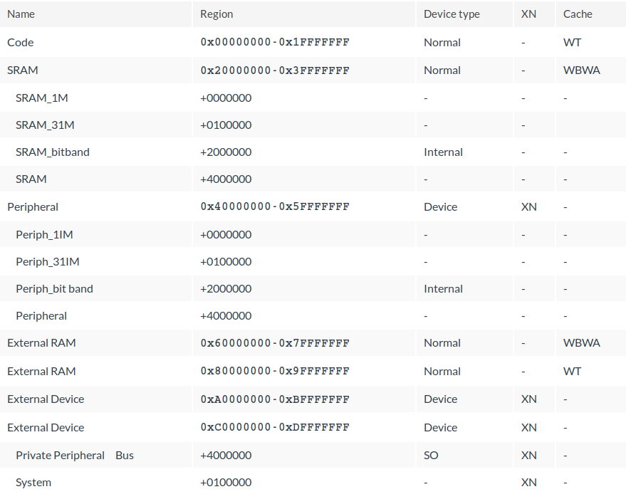
The second solution is to enable the processor's default memory map by setting the PRIVDEFENA flag of the MPU_CTRL register when enabling the MPU:
MPU_CTRL = (1 | 1<<2);
This flag enables a processor-specific background region that might or mighty not be suitable in your case.
This is what it looks like for the Cortex-M3:

As we can see the default map allows read and write access to the whole memory
but sets execution and caching restrictions for some areas.
In most cases that should be a reasonable starting point.
While this is clearly stated in the documentation and should have been obvious I somehow still managed to overlook the issue of alignment in my first test, so I just want to mention it briefly.
The important thing to note here is that for a region to be valid
it has to be aligned to a memory address that is a multiple of its
size.
E.g. a 32k region can start 0x8000, 0x16000, ...
A 512M region can start at 0x20000000, 0x40000000, ...
At some point I was trying to figure out why a region I had configured would not have any effect. While ultimately it turned out to be an alignment issue, at first i suspected that I made a mistake configuring the region as it was not immediately clear to me what the Region Number Register (RNR) and the VALID flag of the Region Base Address Register (RBAR) did and what the difference between them was.
Basically both of them will achieve the same goal and you need to
use only one.
They simply cover different use cases.
The RBAR VALID flag lets you select a region and set its base address in one swoop:
RBAR = 0x10000000 | VALID | 1;
You can do the same thing using the RNR:
RNR = 1;
RBAR = 0x10000000;
But that is not its main use case.
Typically you will set up the region's base address at some time
during startup. That you can do with RBAR VALID.
At a later point you might want to reconfigure a region, e.g. to
let a privileged process write to a read-only area.
For this you can select the region with RNR and then change
only the attribute you are interested in:
RNR = 5;
RASR |= (0x03 << 24) // Allow read/write for all processes
One last thing to note is how the MPU handles overlapping and non-contiguous regions.
While the MPU is only capable of handling a maximum of eight regions overlapping and subregions still allow you to craft rather intricate memory maps and set pretty fine grained access restrictions.
Regions are allowed to overlap.
In such a case the region with the higher ID has priority and eclipses the
lower region.

For example in the depicted case 0x00000010 would be writable while 0x000015000 would be read only.
Additionally every region larger than 128 bytes is always subdivided into
eight subregions of equal size that can be individually enabled or disabled
using the Subregion Disable Bits (SRD) of the RASR register.
Accordingly the SRD field is eight bits wide, 1 means the respective
subregions is disabled, 0 means the subregion is enabled.

In this image SRD for Region 2 is 0b01100000 (0x60). Therefore the subregions at 0x00005000 and 0x00006000 are disabled and access to those areas is governed by Region 1 instead. This means they are writable even though Region 1 has lower priority than Region2.
Finally here is a full example for all the concepts described in this article.
This code configures the MPU regions as shown in the previous picture:
In addition Region 0 is used as the default region covering the whole 4GiB address range and blocking every every access that is not explicitly permitted by the other regions.
#define VALID           (0x10)
#define ENABLE          (0x01)
#define SIZE_16K        (13 << 1)
#define SIZE_32K        (14 << 1)
#define TEXSCB          (8 << 16)
#define NO_ACCESS       (0x0)
#define RW_ACCESS       (0x03 << 24)
#define RO_ACCESS       (0x06 << 24)
#define R2_SRD          (0x60 << 8) // SRD:0b01100000

RBAR = 0x00000000 | VALID | 0;
RASR = ENABLE | TEXSCB | SIZE_4G | NO_ACCESS;
RBAR = 0x00004000 | VALID | 1;
RASR = ENABLE | TEXSCB | REGION_16K | RW_ACCESS;
RBAR = 0x00000000 | VALID | 2;
RASR = ENABLE | TEXSCB | REGION_32K | RO_ACCESS | R2_SRD;