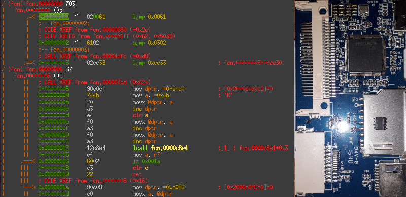

Update June 12 2019: I received some additional information on this chipset that mostly confirms my hunch that it lends itself to exploitation. See details below.
One of the side projects I was working on over the past couple of weeks was reverse engineering the firmware of some USB multi-card readers. Originally I intended to only post a writeup once the project was finished. But Since I decided to lay the project to rest for now due to other obligations I nonetheless present you with my intermediate results in the hope that they will be useful or at least entertaining.
BTW: If you have further information on the Genesys logic chipsets encountered below or even access to the respective SDKs I would be happy to hear from you. That might be just what it takes to encourage me to finish this project ;).
As has been known at least since BadUSB and bunnie's and
xobs' SD card hacks even simple USB devices usually contain relatively
powerful microcontrollers that can be more or less easily exploited. When I had to replace one of my USB multi-card readers due to
some broken pins of the CF slot that was the perfect excuse to take it apart and find out if that applies to this device, too.
Just as expected the card reader contains a CPU and field programmable flash memory and should in theory be exploitable.
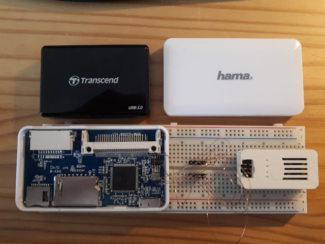
The first step obviously is to take the reader apart. This reveals two easily identified components that might be of interest:
The datashee for the flash chip is easily found on the internet.
The datasheet that is available for the GL3223 controller is somewhat limited. It mostly consists of the description of the chip's physical characteristics, a block diagram of its functional blocks and some high level information.
The most important information found here is that the controller contains a 8051 microcontroller and that the contents of the flash memory can be updated over USB using the "MP Tool" or "Multi-Tool" programming tools.
Armed with the names of the OEM programming tools both applications can be found for download from several Russian and Chinese web sites.
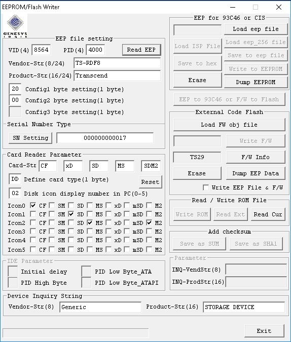
Using those tools the controller's firmware can be downloaded from the device without encountering any additional security measures.
Next the firmware images is loaded into radare2.
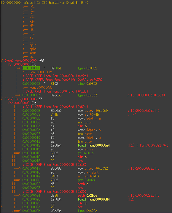
A first glance at the disassembly reveals a short vector table at the start of the binary and what looks like a main loop a little further down.
So it looks like we have a valid 8051 binary here. Well... that was easy.
Before taking a closer look at the firmware it is interesting to know if it is at all possible to replace it with a modified version or if there are any security mechanisms that prevent tampering with it.
Due to the general lack of any security measures up to this point there is no reason to expect any advanced features of that kind like signature verification or other secure boot methods. Nonetheless I proceeded a little more carefully from here on as I didn't want to brick the device on my first try of flashing modified firmware.
Since reading out the firmware was trivial and I had another identical reader at hand I dumped an image of that, too. This allowed me to compare the two images and look for checksums or other properties that might prevent modification of the firmware.
It turned out that the only differences between the images were the serial numbers and two other strings that I presume represent the manufacturing date or lot number.
That gave me some confidence that other areas of the binary also would not be secured by checksums and so I incrementally tried to modify different properties of the image. First the manufacturer string, then the vendor id. Both modified images could be flashed without any problems and worked flawlessly.
Next I became a little bolder and started to make some non functional changes to the code like replacing a couple of instructions with different but functionally equivalent ones. Once more the programming tool and reader accepted the firmware and everything was still working.
So obviously it is possible to flash an run arbitrary firmware images.
I guess that means we have successful code execution. Yay! (Though that was a little too easy to be really enjoyable ;))
To determine where to go from here I took a closer look at the firmware.
First of all I retrieved a third firmware image from another reader I had lying around. This one is from a different manufacturer
and has a different hardware layout but uses the same chipset. While at first the images looked quite different on a closer look they
turned out to actually be rather similar. The majority of code blocks appeared in all of the images although often at different
offsets and sometimes in different order.
I suspect that the images were generated using the same SDK with the differences mainly accounting for differences
in the hardware layout (1 or 2 LEDs, different flash chips, ...).
Also apparent in both images was a structure consisting of mainly two large loops. The first one I presume to be an initialization loop that configures the hardware and probably also handles the flashing (the flashing tool shows the message "enabling boot mode" at some point during the flashing process, so there probably is some control sequence that switches the controller into a bootloader mode). The second loop I suspect to be the main loop that is responsible for the actual data transfer between USB and the memory cards.
At this point it would have been nice to have access to the SDK or at least a datasheet of the particular 8051 core. As I don't currently have access to any of those I continued by writing some code I could inject into the main loop to fuzz the interesting ports and registers so I could find out how to communicate interactively with the device and write a debugger or monitor program for it.
My first attempt was to add a little loop that in turn would set all the 8051's port registers to a high level then wait for a moment and then set them to low. What I expected to find was to see the status LED blink at least once and maybe some level shifts on the USB data lines.
Unfortunately that didn't go quite so well. After flashing the new firmware and resetting the reader the status LED actually did blink 3 times instead of the usual 2 I had observed until then. That gave me some confidence that my approach is generally sound. On the other hand, there was no further response from the device after that point. It was neither visible via USB, nor would the programming tool recognize it any longer :(.
I guess my fuzzing loop must have messed up the communication between the 8051 and the USB controller.
I figured my only option at this point was to flash a working firmware directly into the SPI flash without going through the GL3223 chip.
For this I used a Raspberry Pi and flashrom.
(For detailed instructions check out this article).
First there were some obstacles to overcome, though.
To connect the chip to the Pi's SPI bus I could either desolder it or use a test clip.
I did not have a suitable test clip at hand, but that problem was easily solved thanks to thingiverse
and the magic of 3D printing.
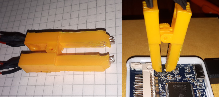
With the freshly printed clip I tried to read the ROM. Unfortunately I did not get any response from the chip. After fiddling around with several parameters of the software and trying different ways to supply power to the chip I suspected a problem with the test clip (which turned out not to be the case). So I soldered a couple of wires directly to the chip.
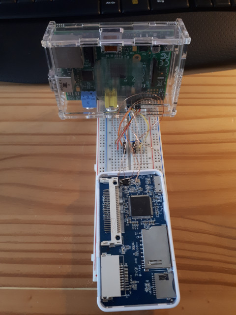
That didn't work either. So the only remaining option was do desolder the chip and connect it directly to the Raspberry Pi's SPI bus (using my new test clip again). That finally was at at least partially successful.
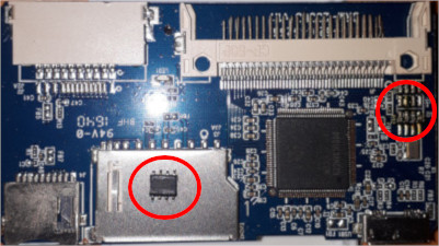
Now flashrom would detect the chip.
I was not yet able to read any data as the ROM type was not supported in the version I was
using. Adding support for the chip to flashrom would not have been a big deal due to the excellent datasheet but it turns out that was not even
necessary as there was already a patch available that did just that. Strangely the vendor and
device IDs didn't match the ones reported by my particular exemplar so I had to change that.
At this point I was finally able to dump the ROM's contents again.
No surprise here, I got back exactly the modified firmware image that I had flashed before and that bricked the device. So all
I had to do now was to use flashrom to write a known good image back to the ROM to get everything working again. After doing
that and soldering the ROM back in place the reader was working again.
So this is where I am at right now.
While the project can not generally be considered a success, I do believe that it proofs that "dumb" devices like USB card readers can serve as an attack vector. Due to the fact that the device's firmware can be modified without any modifications to the hardware and that the chipset is powerful enough to allow additional functionality to be implemented, an attacker with sufficient resources and possibly access to OEM documentation and tools would probably be able to modify such a device to inject malicious data and use this as an entry vector to gain access to sensitive information.
If you have any further questions or comments, please do not hesitate to contact me. Any feedback is greatly appreciated.
I recently received some additional information on the chipset from someone who would like to stay anonymous. Therefore I will only post a short summary here to prevent any unintentional disclosure of personal information.
First of all I got some additional datasheets. Unfortunately they do not cover the actual 8051 or USB/Card controller cores but mostly the EEPROM data layout and some configuration information for the chipset. So there is not a lot of information in them that was not already to be learned from the flashing tool.
As for the flashing tool: It seems that what is advertised as an "SDK" is actually not much more than the flashing tool that I already found myself. The tool can generate configuration data to be stored in the EEPROM that can change the behavior of the controller in a couple of limited ways, e.g. select the number and types of card interfaces, set transfer speeds and enable or disable some of the more esoteric features of the various card protocols.
The actual 8051 firmware appears not to be intended to be modified by OEMs. The similarities (and differences) between the images for readers from different OEMs that I encountered are therefore not as I expected due to customizations made by those OEMs but rather a symptom of the ongoing development of the firmware by the chipset manufacturer. (Which makes sense as on closer inspection one of the firmware samples is significantly more complex than the others and shows signs of deliberate refactoring like code blocks with identical functionality that have been broken up into several functions.) I guess that means no SDK for exploit development for me :(.
On the bright side though the informant told me that my ideas about intercepting the data stream between the USB and card interfaces sound plausible.
They suspect that injecting macros into MS Offices files might be stretching the controller's capabilities a little to far, but serving virtual files
containing shellcode should probably be doable.
Since there seems to be no shortcut to exploitation and I currently just don't have the time to dive deep into the firmware I probably won't pursue this project any further, but it certainly is nice to know that my hunch with this thing was correct and we should be careful about blindly trusting "dumb" devices.